EEI Services / Electronic Design Service / Electronic Circuit Board Assembly Service (PCB Assembly)
PCB Assembly Service
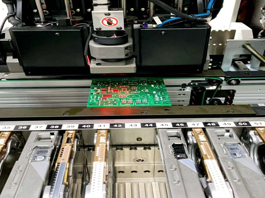
For the assembly of the PCB by using a machine that has high precision in small lots and big lots with Surface Mount Technology (SMT) supported small devices (01005 inches or 0402 mm) by customer supply the component or using our company supply from domestic or abroad.
Scope of Assembly Services
- The assembly line supports the single-side and double-side design.
- Supports PCB sizes from 50mm × 50mm up to a maximum size of 450mm × 400mm.
- Supports PCB thickness from 0.8mm to 2.3mm
- Stencil support with 3 size 550mm ×650mm (21.65” ×25.59”), 650mm ×550mm (25.59” ×21.65”) and 736mm ×736mm (28.97” ×28.97”)
- Able to be tested by following customer’s needs.

PCB Assembly Steps
- The customer forwarded data files for assembly and manufacture including Gerber, NC Drill, Pick and Place, BOM and Assembly Drawing.
- The Electronic Design Center (EDC) checks data files and makes a quotation in 1-5 days excluding weekends and national holidays.
- Order confirmation and payment in term condition.
- EDC orders the production of PCB, Stencil and procurement of electronic components or customer supplies.
- EDC checks PCB and Components that are ready for assembly the PCB.
- EDC assembles the SMD components by machine and through hole.
- EDC testing and checking the quality.
- EDC packing and delivery to customers.
Printed Circuit Board Assembly (PCBA) Technology
1) Surface Mount Technology (SMT): This technology for assembly Surface Mount Device (SMD) that can use a small component for assembly by the machine is sensitive to arrange that such as resistor or transistor by machine will place automatically.
2) Thru-Hole Technology (THT): The THT is the technology for assembly the of components that have a pin inserted into a hole on the PCB with a soldering pin in another side of the PCB this one is used for a large component as a capacitor, relay or terminal block.
PCB assembly process steps
- Solder Paste Stencil: The Stencil uses thin stainless steel with a stencil and is placed on the PCB that can use the solder in some parts of the PCB that is required. After removing the stencil, the solder will be remaining in the position.
- Pick and Place: Place the SMD on the PCB in the direction of XY for placing the component.
- Reflow Soldering: Welding of the device on PCB by heating will make the solder melt and harden for connecting to SMD with PCB.
- Inspection and Quality Control: Common quality checking process.
- Manual Check: Inspecting by eye this method will be efficient in small batches.
- Automatic Optical Inspection: Inspection by using light by this method is used in large batches.
- X-ray Inspection: X-rays are mostly used in PCB that have multilayers that are useful to see each layer and that help to identify the invisible problem.
- Through-Hole Component Insertion: The PCB might have other components without a normal SMD. So that another solution is Plating Through a Hole (PTH) for the PTH needs special soldering in the process of assembly of the PCB.
- Manual Soldering: The common method to set the component into PTH and soldering with soldering iron.
- Wave Soldering: Commonly used in industrial settings by setting the component into PTH after that the PCB will be placed on the conveyer belt by passing through the soldering oven or reflow oven and the machine melts the solder at the bottom plate of the PCB so the solder will be flow on every PTH spot at the same time.
- Final Inspection and Functional Test: Testing the function of the PCB and checking the characteristics of electrical such as voltage, current, signal output, etc.

Contact us
Electronics Design Laboratory (EDL)
B Floor, The Knowledge Exchange: KX 110/1 Krung Thon Buri Road, Bang Lamphu Lang, Khlong San, Bangkok 10600
Mr. Panumas
e-mail : panumas@thaieei.com
Tel : 0 2280 7272 ext. 8335
Miss Orawan
e-mail : orawan@thaieei.com
Tel : 0 2280 7272 ext. 8336