EEI Services / Electronic design services / Electronic circuit board design service (PCB Design)
PCB Design Service
For designing the electronic circuit single-side, double-side or multilayer following the requirements and conditions of the customer by using a program that is accepted worldwide according to standard of design, standard of production or product specifications as an Electromagnetic Compatibility (EMC) including PCB design that have IoT functions for Smart Farm, Smart Home or healthcare applications.
Information for Designing PCB
- The idea for designing the PCB or Block diagram.
- Draft the electronic circuit in handwriting or digital file to make sure that supports to design.
- Data or Datasheet of each component that is used in the design.
- Requirements for designing such as the size of PCB, wiring scale, number of layers, design rule, PCB guideline, or other requirements.
PCB Design Steps
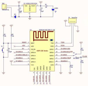
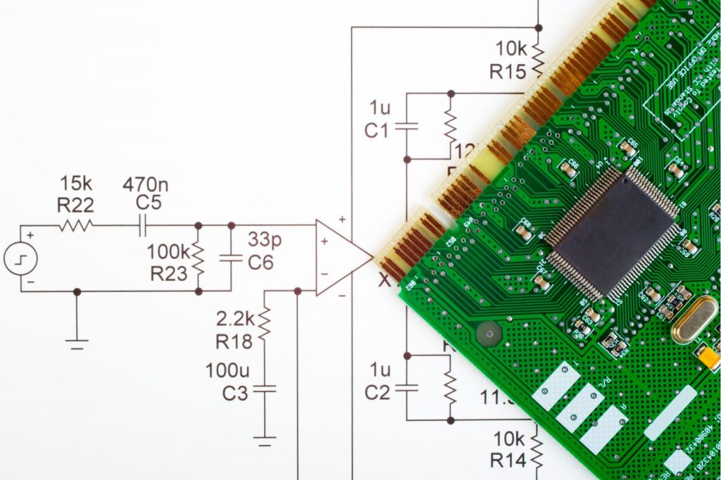
- Schematic Design: Building a block diagram to show all electronic components and routes together.
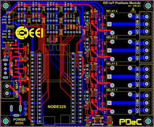
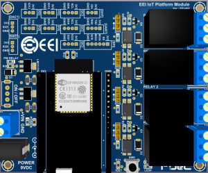
- Board Layout: Creating a layout for importing the component or device (footprint) from the schematic to arrange the components that can wire signal lines connecting.
- Material Selection: Choosing the component that suits for PCB by considering each factor such as heat transfer efficiency, insulator and durability.
- Layer Planning: The planning of the number of copper layers determined by the circuit. Complexity might have many signal lines, so the number of copper layers and arrangement of components was an important step.
- Trace Routing: Designing the connection path on the PCB to connect each component and the complex circuit design of signal lines considering electromagnetic interference and electromagnetic compatibility (EMI/EMC).
- Component Placement: The arrangement of electronic components is one of the keys to making an efficient PCB and making sure that easy to manufacture and assemble.
- Testing and Validation: Simulate the design of PCB to check a problem that might occur as a short circuit, signal integrity or electromagnetic interference.
- Manufacturing file Preparation: The preparation file for manufacturing and assembly is included with the requirement.
– Gerber files for manufacturing the PCB.
– NC Drill files for drilling the PCB.
– Bill of Material (BOM) files for supply and order electronic components.
– Pick and Place files for details of XY and locate each component for use with the machine.
– Assembly Drawing details of position and direction of the component.
** Details of the manufacturing file mentioned above are just one part of the manufacturer and assembly of the PCB that depends on the industry has technology.

Contact us
Electronics Design Laboratory (EDL)
B Floor, The Knowledge Exchange: KX 110/1 Krung Thon Buri Road, Bang Lamphu Lang, Khlong San, Bangkok 10600
Mr. Panumas
e-mail : panumas@thaieei.com
Tel : 0 2280 7272 ext. 8335
Miss Orawan
e-mail : orawan@thaieei.com
Tel : 0 2280 7272 ext. 8336